


22 Apr, 2025
Inside the Manhattan Project-scale effort to rebuild US chips capacity

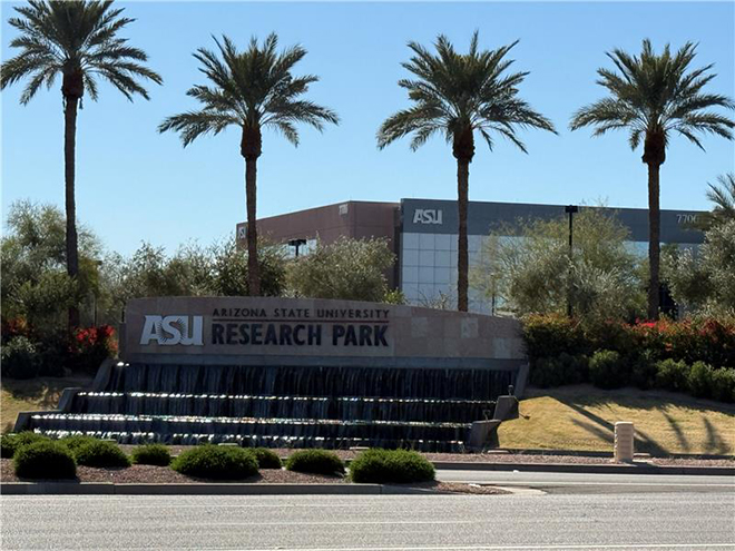
| The ASU Research Park, home to research and development hub Macro Tech Works, will soon house a Chips for America flagship R&D facility. Source: Stefan Modrich/S&P Global Market Intelligence. |
Twenty minutes outside of Phoenix, a former Motorola facility has become the training ground for an emerging generation of US semiconductor workers.
Here, at Arizona State University's Research Park, MacroTechnology Works leases space in its 250,000-square-foot facility to chip companies including Applied Materials Inc., EV Group and ON Semiconductor Corp. In addition to its specialized facilities, the site offers companies access to a talent pool of 29,000 students at ASU's Fulton School of Engineering, some of whom may decide to join the next wave of high-skilled workers designing and producing leading-edge silicon.
The ASU site, which is directly aimed at helping to onshore more US chip manufacturing, has attracted support from both the Biden and Trump administrations. In late 2024, the Department of Commerce announced a $100 million award to the university and Deca Technologies Inc. for the Substrate-based Heterogeneous Integration Enabling Leadership Demonstration initiative, or SHIELD USA. The initiative focuses on developing a domestic advanced packaging ecosystem. Then in early 2025, the Commerce Department awarded $1.1 billion to Natcast — the operator of the National Semiconductor Technology Center — for a prototyping and advanced packaging piloting facility that will be located at the Research Park. The facility, which is set to be operational in 2028, will allow researchers and industry leaders to develop and test new materials, devices, and advanced packaging processes.
The grants flow from $50 billion in funding authorized by the 2022 CHIPS and Science Act, which is intended to revitalize the US semiconductor industry. While President Donald Trump has criticized the CHIPS Act in the past, at the end of March, Trump issued an executive order setting up the United States Investment Accelerator, a new entity within the Commerce Department that will take over the CHIPS Act program. The Investment Accelerator is tasked with facilitating and accelerating investments of more than $1 billion.
"If the US can continue funding and continue incentivizing not only manufacturing here in the US, but also that innovation pipeline, that's where we win," said Jason Conrad, COO of the SWAP Hub and ASU Knowledge Enterprise. "That's where we get the advantage over our adversaries and get ahead."
Closing the talent gap
It's a costly endeavor, as evidenced by the size of the funding grants. ASU President Michael Crow pointed to the $1.1 billion Natcast research and prototyping facility as a prime example.
"This is the largest of three CHIPS R&D flagship facilities being launched that together represent the greatest national laboratory investments since those that came out of the Manhattan Project," Crow said.
The parallels between the Manhattan Project and the CHIPS Act do not end at the nexus of government and academia. The bipartisan sense of urgency in Washington to jump-start domestic chip production extends to the training of engineering students who are needed to fill roles across the industry.
The Semiconductor Industry Association projects the industry's workforce will grow by nearly 33%, or 115,000 jobs, by 2030. That would bring the total workforce to 460,000 jobs in five years. But due to a lack of skilled workers, nearly 58% of the new jobs — or about 67,000 — are at risk of going unfilled.
"We're producing 7,000-plus graduates a year in engineering, and we get told by our partners all the time that it's not nearly enough," said ASU's Conrad, who has more than two decades of experience at companies like NXP Semiconductors NV, GlobalWafers Co. Ltd. and Lam Research Corp.
The skilled labor shortage is a major topic of conversation across all levels of the chipmaking industry.
"Every single time we go to a customer … it always comes to a conversation about workforce," said Craig Bishop, chief technology officer at Deca Technologies. "Where are we going to hire trained engineers? Or if we have engineers, where can they train to come up to speed on new technologies? And that's where ASU is now our de facto answer for those questions."
In addition to providing students with hands-on experiences, MacroTechnologyWorks also makes innovation more cost-effective and scalable for smaller industry players, Conrad said.
"Small businesses can't afford to do a clean room, they can't afford to have all the equipment that it requires to make their prototypes," Conrad said. "We have up to 10 small businesses renting here at any one time, they rent their small footprint at cost, and then they leverage the entire site and the assets that we have to advance their innovation and make it faster to get to market and be able to continue to innovate at a reasonable and lower cost than it would be possible to do on their own."
|
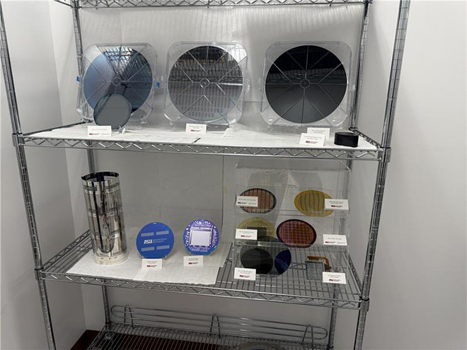
MacroTechnology Works — a 250,000-square-foot facility with a 49,000-square-foot clean room and specialized tools for R&D, prototyping and semiconductor manufacturing — produces silicon wafers like those shown here. |
'An inflection point'
With Deca's emphasis on advanced packaging, its role in the industry is to bring its technologies to other companies and help them scale up their manufacturing operations, Bishop said.
Several steps lead up to the advanced packaging stage of chip manufacturing, including the extraction of silicon and other raw materials used in more specialized chips. Once the silicon is melted and sliced into thin wafers, they are polished to ensure a smooth surface for the subsequent steps in the manufacturing process, including etching and purification.
The wafers are then tested, diced into individual chips, and packaged into protective casings that facilitate connections to other electric components.
"For decades, we got away with scaling down and putting more things into one piece of silicon, one chip, but now you can't do that anymore," Bishop said. "Especially for things like AI chips or the large, high-performance chips that power supercomputers or ChatGPT. Everything has to be split across multiple chips and put back together with advanced packaging, kind of stitching together the smaller chips to make larger functional devices. And it's a huge change technology-wise. … It's an inflection point in the history of semiconductors."
The shifts across the industry extend beyond manufacturing to how NVIDIA Corp. and Advanced Micro Devices Inc. have adapted their designs to reflect that rise of advanced packaging, at a moment ripe for ASU and its partner institutions across the SWAP Hub to become powerhouses of R&D.
"It's exactly the right time to do this, because we need a new center of innovation for this, what industry calls advanced packaging," Bishop said. "It's the new way to make chips."
'A broader supply chain win'
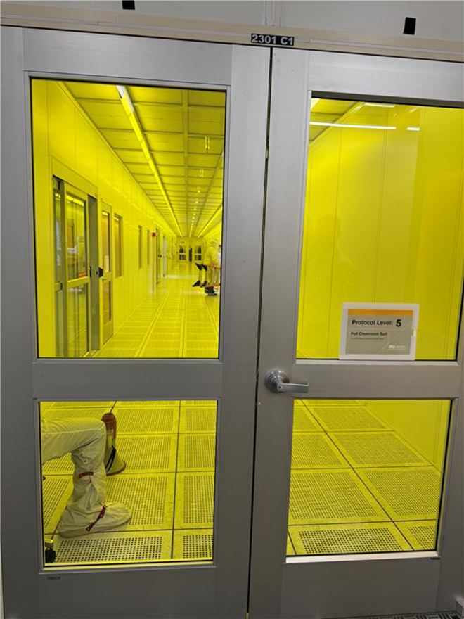 Strict protocols are observed inside the clean room at Macro Tech Works to ensure a contamination-free environment for sensitive research and manufacturing processes. Strict protocols are observed inside the clean room at Macro Tech Works to ensure a contamination-free environment for sensitive research and manufacturing processes. |
There is a circular quality to the formula of ASU officials working in concert with local, state and federal authorities and their industry partners.
Phoenix Mayor Kate Gallego, whose first international trip as mayor was to help recruit Taiwan Semiconductor Manufacturing Co. Ltd. to expand its operations to the region and who assisted in pushing for Intel Corp.'s expansion in the Phoenix metro area, told Market Intelligence ASU was essential in securing the commitment from TSMC to break ground in Arizona.
"TSMC is making investments in technology we don't have in the US today," Gallego said. "They need a university that will help them develop a leading-edge workforce, and ASU is very good at understanding business needs and crafting education programs for their graduates to hit the ground running."
In 2023, Phoenix voters approved $500 million in general obligation bonds, a portion of which will go toward expanding the university's presence in the city.
In March, TSMC said it intended to spend an additional $100 billion to expand its US semiconductor manufacturing, bringing its total investment in the US to $165 billion. TSMC's expansion plans include three new fabs, two advanced packaging facilities and an R&D team center. If realized, TSMC's spending would represent the largest foreign direct investment in US history.
TSMC told its investors on an April 17 earnings call that its first fab in Arizona began high-volume production at the end of 2024, yielding results comparable to its Taiwan fabs. TSMC Arizona Corp.'s construction of a second fab is already complete, TSMC CEO C.C. Wei said on the call, while construction on a third and fourth fab is set to begin later this year. Construction of a fifth and sixth fab, which Wei said will use "even more advanced technologies," will be based on customer demand.
"After completion, around 30% of our 2-nanometer and more advanced capacity will be located in Arizona, creating an independent leading-edge semiconductor manufacturing cluster in the US," the CEO said. "It will also create greater economies of scale and help foster a more complete semiconductor supply chain ecosystem in the US."
AMD on April 14 announced its fifth-generation processor chips would be built at TSMC's Arizona facility.
TSMC's success, in a sense, is a collective win for the industry and the private-public partnerships that made it possible, Bishop said.
"It's a broader supply chain win," Bishop said. "If they didn't have offices here before, they do now, and if they didn't have labs here, they do now, because it's such a locus. We operated a factory in Asia for years, and we used to travel to all the different suppliers across Asia, Europe, and others. Now, more and more of our suppliers are located near us and come to visit us in Arizona. So it has been a really big shift just in the last few years."